Computed tomography
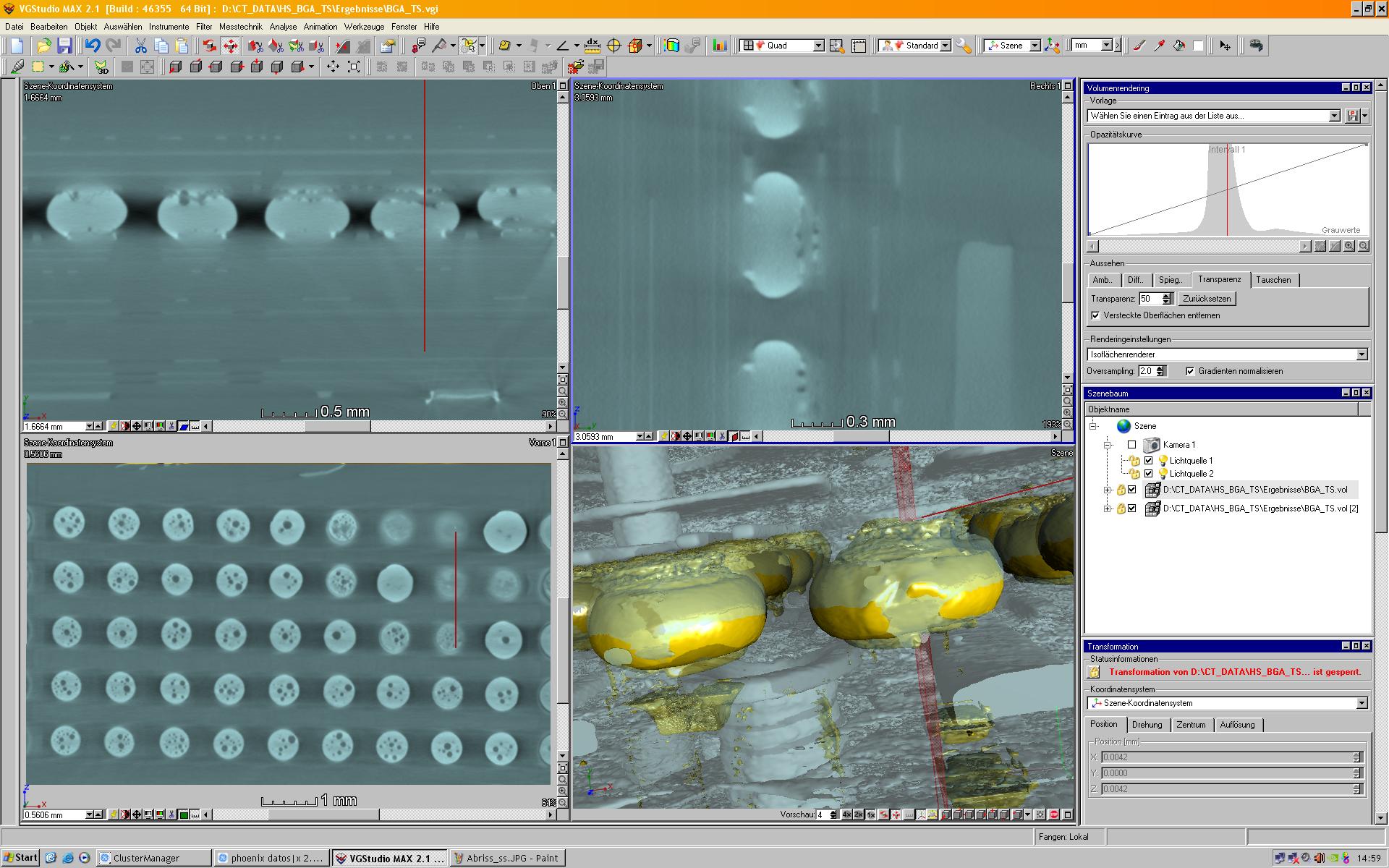
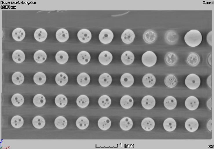
In the Laboratory for Assembly and Joining Technology at Hochschule München, objects ranging in size from less than 1 millimetre to approximately 120 mm can be examined using a computerised tomography scanner.

Using the image processing software, these objects can be analysed and measured in both 2D and 3D views. We will also provide you with a measurement report.
Technical specifications
- X-ray source: maximum voltage/power 180 kV/15 W
- Target: Tungsten on beryllium or molybdenum
- Geometric magnification: 1.7× – 250×
- Resolution: up to 200 nm (0.2 µm)
- Minimum voxel size: up to 500 nm (0.5 µm)
- Detector: High-Contrast Detector HCD 120-50, 12-bit/16-bit, 3-fold measurement range extension (max. 6,900-pixel detector width)
- Pixels: 2,300 x 2,300
- Pixel size: 50 µm
- Max. sample diameter: < 1 mm to 120 mm
Applications of CT
- Insights into objects and assemblies
- Damage analysis
- Checking connections
- Dimensional measurement technology
- Volume analysis
- Target versus actual comparisons
- Detection of defects, e.g. cavities, pores or foreign particles
- Determining precise information about shape and position
Insights into objects and assemblies

A glimpse inside a torch with a broken solder joint.

An insight into a high-frequency filter
Damage analysis

Fault Analysis
: Using a computerised tomography scanner, we can inspect printed circuit boards and components for short circuits or open circuits.

Three-dimensional measurement technology
: 3D coordinate measurement technology enables workpieces to be measured and dimensioned in both three-dimensional and two-dimensional views.

Volume measurement
: Using CT, we can, for example, carry out volume measurements.

Target-Actual Comparison
: Using CT, we can compare components with a reference sample and check that manufacturing tolerances are being met.
Cross-section preparation technique

Using the cross-section preparation technique, we can examine various material samples and electronic components. To do this, the samples are embedded in a suitable medium, ground, polished and then analysed using a stereo magnifier and a microscope.
Technology
Offers:
- Prototype manufacturing using thick-film hybrid technology
- Shear and tensile tests for test series
- Replacement of components on printed circuit boards
- Thick-wire and thin-wire bonding for experimental purposes
- Flip-chip bonding
- Training courses